


Before now and from now.
Together with the evolution of a connected society through advanced material technologies.
About EMBD
Panasonic Industry Co., Ltd. embodies the concept of "Transforming the world you see from places you can’t see." by developing a variety of electronic devices and materials in the three fields of Automotive CASE, ICT infrastructure, and Factory Automation.
Electronic Materials Business Division being a part of Panasonic Industry is the only entity in the Panasonic Group specializing in materials. We will support the evolution of a "connected society" together with customers around the world through electronic materials developed from advanced material technologies, originated from the "Nerimono (resin synthesis)" technology at the time of our founding.
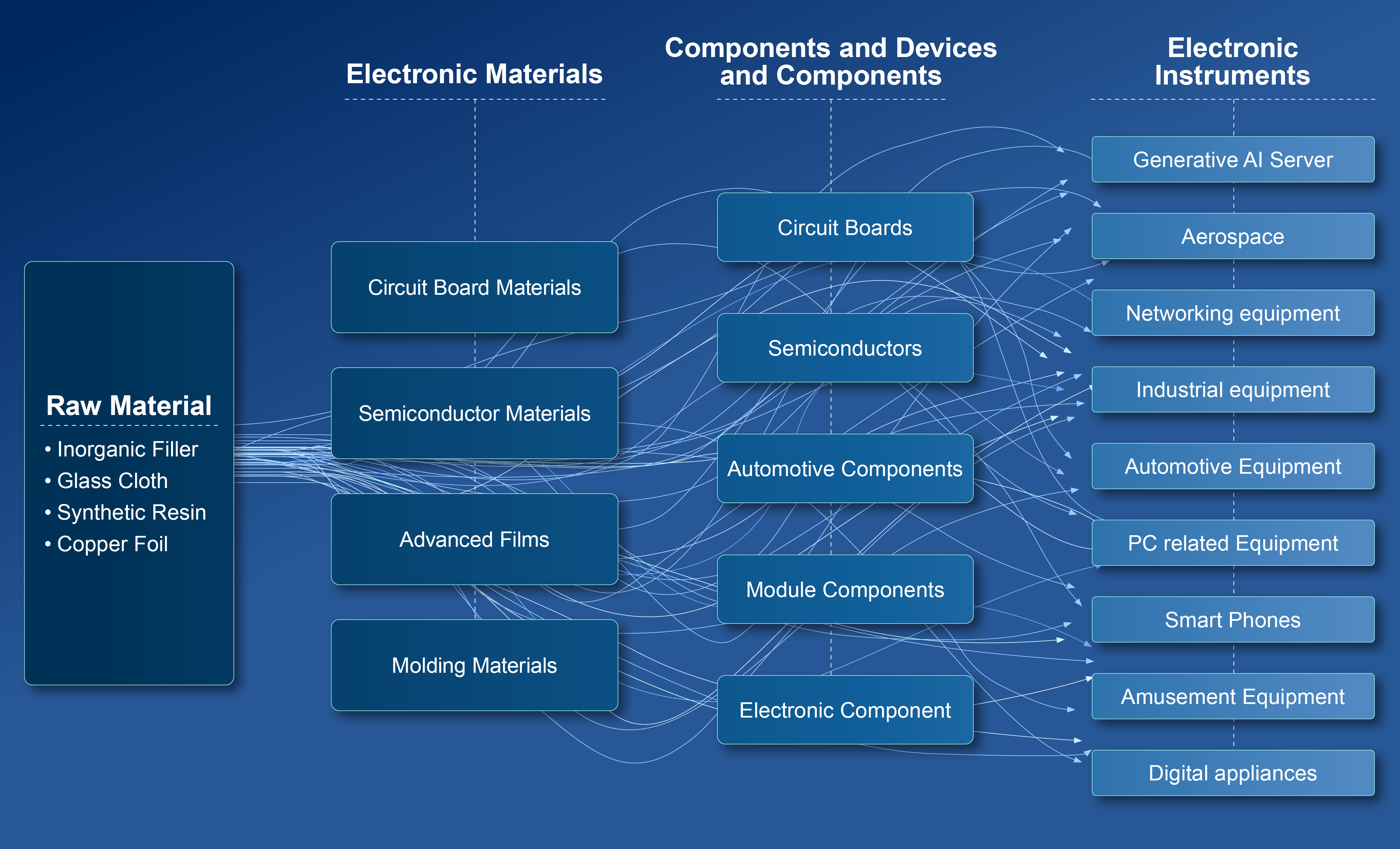
Our Business Field
Electronic materials are used in semiconductors, electronic circuit boards as composite materials composed of various raw materials.
They play active roles in a wide range of fields, including ICT infrastructures, automobiles, and satellites.
Our Contribution to Generative AI
Generative AI has now become indispensable to us. Generative AI, now we cannot live without.
The evolution of data amount being computed and those processing speed are unstoppable, and the number of AI servers to be processed is expected to increase to 240% in 2028 compared to 2024.
These are supported by our company's MEGTRON series of low-transmission loss multilayer substrate materials. Our company's MEGTRON series of low transmission multilayer substrate materials support those processes.
Contributing to further technological innovation and market expansion of generated AI. MEGTRON series contribute to further technological innovation and market expansion of generated AI.

Panasonic Industry will Double the Production Capacity of MEGTRON Multi-layer Circuit Board Materials Over the Next Five Years
Panasonic Industry Announces an Investment of 7.5 Billion yen for a New MEGTRON Circuit Board Materials Production Line to Address Growing AI Server Demand
Products of EMBD
Circuit Board Materials
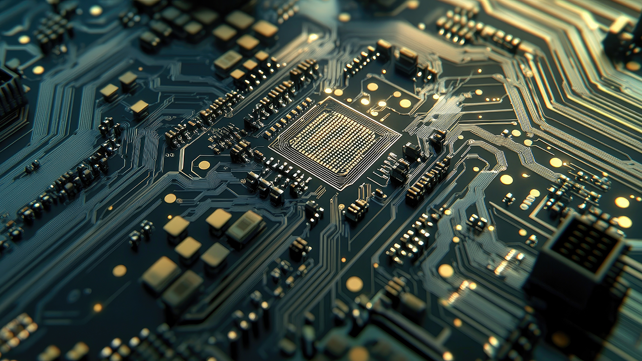
Our Circuit Board Materials are used in a wide range of applications around the world, contribute to high speed and high-capacity generated AI servers and mobile phone base stations, and support the functionality and reliability of electronic devices.
Semiconductor Device Materials
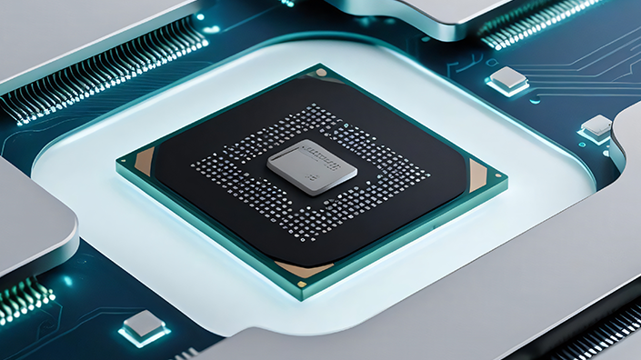
Semiconductor Device Materials include substrate materials of semiconductor package form the basis of semiconductors, encapsulation materials protects semiconductors from harsh environments, and materials that reinforce packaging. There are substrate materials of semiconductor packages form the basis of semiconductors, encapsulation materials protects semiconductors from harsh environments, and materials that reinforce packaging.
These materials play an important role in improving performance and ensuring the reliability of semiconductor devices.
Plastic Molding Compounds
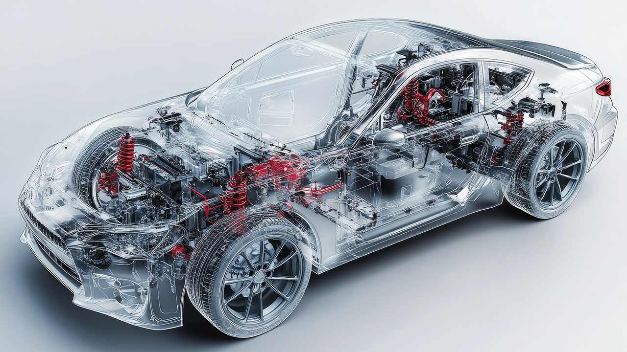
Plastic Molding Compounds are raw materials for plastic products. There are thermosetting resins that harden by heat and thermoplastic resins that can be molded by reheating, and used in a wide range of fields, such as in-vehicle equipment and home appliances.
Advanced Films

Advanced Films are materials that have surface functions to meet diverse needs.
We have lineups of HUD cover films that are used for display devices in automobiles to prevent temperature rise, malfunction, and loss of visibility due to direct sunlight, and various films that prevent iridescence, and reflection.