Measure for protecting in-vehicle Ethernet against ESD, using a high-tolerance ESD suppressor
2022-11-23
- Anti-ESD circuit defined by the Open Alliance (in-vehicle Ethernet standardization body)
- ESD protection element specifications and required tests specified by the Open Alliance
- Evaluation results of a high-tolerance ESD suppressor subjected to a required test defined by the Open Alliance
- Conclusion
- Related product information
- Related information
- Tags related to this article
The number of cars equipped with an in-vehicle electronic control unit (in-vehicle ECU) is expected to increase as driving assist technologies advance and communication electronic equipment becomes widespread. In-vehicle electronic control units incorporated in cars will increase communication loads that in-vehicle networks have to handle. An in-vehicle Ethernet is a promising system that allows large-capacity and faster in-vehicle network communications. It achieves a data transmission rate higher than that of a CAN and is capable of data exchange conforming to the IP (internet protocol). The system offers some advantages, such as ease in utilizing commercial Ethernet technologies and high security features. This article shows readers evaluation results of how a high-tolerance ESD suppressor is an effective measure for protecting in-vehicle Ethernet against ESD.
Anti-ESD circuit defined by the Open Alliance (in-vehicle Ethernet standardization body)
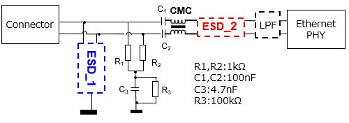
Open Alliance, an in-vehicle Ethernet standardization body, defines the layout of ESD protection elements shown in the following diagram (Fig. 1). As an anti-ESD component configuration, you can choose either a configuration in which ESD_1 is disposed underneath a connector or a configuration in which ESD_2 is disposed between a common-mode choke coil (hereinafter "CMC") and an Ethernet PHY (physical layer IC). The previously presented article "Measure for protecting an in-vehicle LAN (Ethernet) against ESD" introduced a circuit configuration in wide use in which ESD_2 is provided with a TVS diode. Currently, however, a circuit having an ESD protection element incorporated in the ESD_1 located close to an ESD input unit is in wide use. Note, however, that the Open Alliance defines specification requirements and test items for the ESD protection element incorporated in ESD_1.
ESD protection element specifications and required tests specified by the Open Alliance
In Ethernet communication, a trigger voltage (operation start voltage) to the ESD-1 is 100 V or higher, which far exceeds an operation start voltage of 27 V or higher to an ESD protection element (laminated varistor or TVS diode) used as an anti-ESD measure in CAN communication. Ethernet communication, therefore, requires generation of a high trigger voltage. Panasonic's high-tolerance ESD suppressor meets specification requirements for the ESD protection element listed in the following table, defined by the Open Alliance.
In the following section, we will discuss the evaluation results of the high-tolerance ESD suppressor which was subjected to a required test for an ESD protection element, being shown in table 2.
| Item | Specification requirements | High-tolerance ESD suppressor |
|---|---|---|
| Polarity | No polarity (bidirectional) | No polarity (bidirectional) |
| Allowable circuit voltage (Vdc max.)(Vdc max.) | 24 V DC or higher | DC 50V max. |
| ESD trigger voltage | 100 V or higher | 400 or higher (typ.) |
| ESD resistance | 150pF/330Ω ±15kV | 1150pF/330Ω ±25kV (typ.) |
| Number of times of ESD application | 1000 times or more (IEC level 4) | 1000 times or more (IEC level 4) |
| No. | Test item | Test objective | Test summary |
|---|---|---|---|
| 1 | Mixed Mode S-parameter measurement |
Evaluating the quality of a differential signal | Measuring S-parameters (Sdd11, Sdd21, Ssd21) |
| 2 | Damage from ESD | Evaluating the signal quality at the time of ESD application | Measuring S-parameter fluctuations before and after ESD application |
| 3 | ESD discharge current measurement | Evaluating an ESD current that flows through Ethernet PHY when an ESD protection element is used | Evaluating a current that flows through Ethernet PHY in a circuit including an ESD protection element, a termination circuit, and a CMC in a simulation test |
| 4 | Test of unwanted Clamping Effect at RF immunity Tests |
Evaluating RF immunity at the application of an RF voltage | Evaluating S-parameter fluctuations that occur when a voltage higher than a reference voltage is supplied |
Evaluation results of a high-tolerance ESD suppressor subjected to a required test defined by the Open Alliance
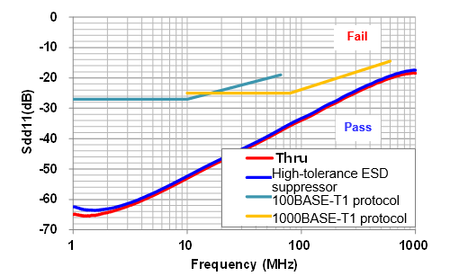
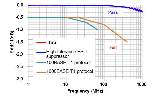
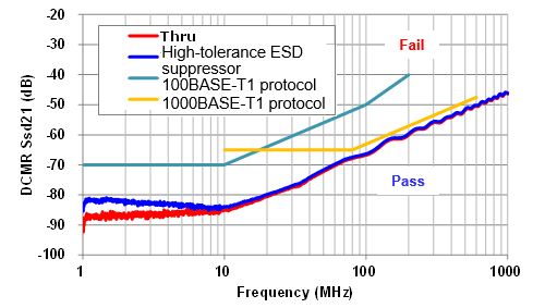
1. Mixed Mode S-parameter measurement
To evaluate the signal quality, the following three S-parameters are measured.
(1) Sdd11 (return loss): The amount of reflection of an input differential signal at the input end
(2) Sdd21 (input loss): The amount of loss of an input differential signal at the output end
(3) Ssd21 (signal mode conversion): The amount of conversion of an input differential signal into a common mode signal at the output end
Regarding Sdd11 and Sdd21, it is known that an increase in the difference between the capacitance of the ESD protection element and the capacitance of a capacitor paired with the ESD protection element leads to the degradation of Ssd21 (signal mode conversion).
The high-tolerance ESD suppressor with a small capacitance of 0.1 pF and a narrow tolerance of +0.1/-0.08 pF ensures a high signal quality and meets the specification requirements.
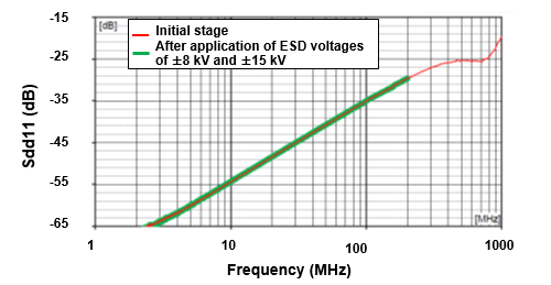
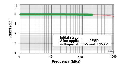
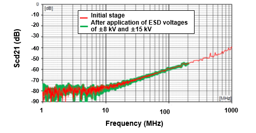
2. Damage from ESD
<Procedure for evaluating S-parameter fluctuations caused by ESD application>
(1) Measure the initial values of the S-parameters (Sdd11, Sdd21, Scd21), i.e., S-parameter values before ESD application.
(2) Apply IEC61000-4-2 contact discharge noise ±8 kV 20 times→ S-parameter measurement
(3) Apply IEC61000-4-2 contact discharge noise ±15 kV 20 times→ S-parameter measurement
<Criteria>
Fluctuations of Sdd11 and Scd21 (signal mode conversion at four ports), i.e., a difference between Sdd11 and Scd21 before ESD application and Sdd11 and Scd21 after ESD application, remain within ±1 dB.
Fluctuations of Sdd21, i.e., a difference between Sdd21 before ESD application and Sdd21 after ESD application, remain within ±0.1 dB.
For example, an ESD protection element with low ESD tolerance shows a great change in S-parameters caused by degrading insulation properties, thus becoming incapable of meeting mixed mode S-parameter standards indicated in 1. With an ESD tolerance of 25 kV, the high-tolerance ESD suppressor meets the above criteria for S-parameter fluctuations caused by ESD application.
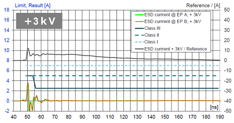
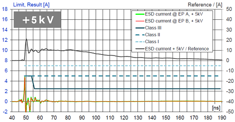
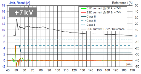
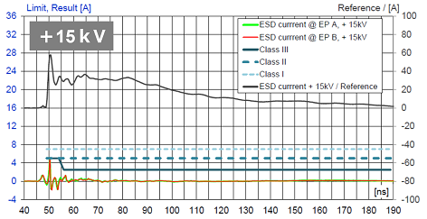
3. ESD discharge current measurement
To evaluate S-parameter fluctuations, only the ESD protection element is analyzed. On the other hand, in an ESD discharge current test, an actual circuit simulated shown below is analyzed. Impedance that arises when a PHY operates is simulated as 2 Ω resistances at the rear stage of a CMC, and current flowing to the PHY is analyzed from a waveform appearing on an oscilloscope.
The Open Alliance standard sheet classifies ESD protection elements into a Class I element, Class II element, and a Class III element based on current flow to the PHY. The Class III element is the ESD protection element with the best anti-ESD performance.
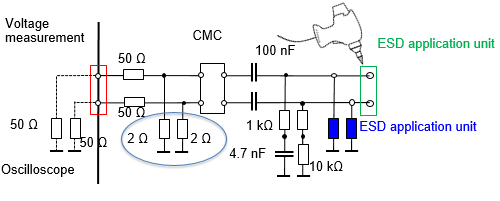
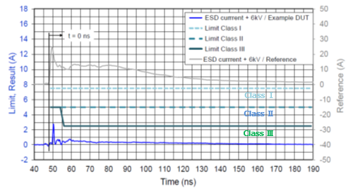
Fig. 6 shows current waveforms that result when ESD voltages of 3 kV, 5 kV, 6 kV, 7 kV, and 15 kV are applied to a circuit that includes the high-tolerance ESD suppressor and the CMC for 100BASE-T1 Ethernet. Each current waveform shows that its wave peak reaches a point close to 5 A, which is the limit value of the Class III element, but the current value following the peak remains almost 0 A, which indicates that a leak current to the PHY is suppressed. Applying an Increase to the ESD voltage barely causes a waveform change, which demonstrates that the high-tolerance ESD suppressor suppresses the leak current to the PHY. The Class III ESD suppressor element is the best among the Class I, Class II, and Class III elements.
4. Unwanted Clamping Effect at RF immunity Test
In this test as the same as in the ESD discharge current test, not the ESD protection element itself but a circuit including a combination of the ESD protection element and the CMC is analyzed (Fig. 7). This test is conducted to verify whether the ESD protection element clamps noise when an RF-generating voltage is applied to the circuit. The ESD protection element needs to suppress fluctuations of common mode rejection (CMR) caused by the application of a voltage higher than a reference RF-generating voltage to keep the fluctuations within ±1 dB relative to CMR that results from application of the reference RF voltage. CMR is given by the following equation.
CMR = P_in - P_out
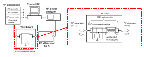
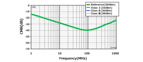
Fig. 8 is a graph showing evaluation results of the RF immunity of the application of the RF voltage. The graph demonstrates that the CMR does not change when an RF voltage of a 39 dBm level (Class III level) against a 20 dBm level (reference voltage) is applied to the circuit. This indicates that the high-tolerance ESD suppressor has high immunity to RF voltage application.
Conclusion
In this article, we have introduced the specification requirements and test items for the ESD protection element defined by the Open Alliance, an organization that promotes standardization of the in-vehicle Ethernet (a promising in-vehicle communication network) and reported evaluation results of various test items for the high-tolerance ESD suppressor developed by Panasonic. The high-tolerance ESD suppressor has been certified by a third party certification body (FTZ) that it meets specification requirements for the 100BASE-T1 Ethernet and will serve as an effective measure for protecting in-vehicle Ethernet against ESD.
Related product information
Related information
- ESD Controls for Automotive LAN (Ethernet)
- Noise-reducing measures start with knowing about the different types and properties of noise.
- Basics of Surge/ESD and Protection Components
- Common Mode Noise of High-Speed Differential Data Transmission and Management of Internal Interference to Wireless communications
Tags related to this article