BCI Testing and Communication Errors: Impacts of ESD Protection Devices and Countermeasures
2025-12-24
- What Is BCI Testing?
- Mechanisms Behind Communication Errors During BCI Testing
- Examples of Communication Errors Caused by ESD Protection Devices
- Mechanism of the Reverse Recovery Phenomenon in Zener Diodes
- Differences Between Zener Diodes and MLCVs Based on V-I Characteristics
- Key Considerations for Selecting and Designing ESD Protection Devices
- Features of Automotive CAN-FD-Compatible 2-in-1 Chip Multilayer Ceramic Varistors
- Summary
- Related Product Information
- Related Articles

As high-speed automotive communication technologies such as CAN-FD and Automotive Ethernet become increasingly widespread, the risk of communication errors caused by external noise is also growing. Chip multilayer ceramic varistors (MLCVs) and TVS diodes (including those based on Zener diode structures) are commonly used as electrostatic discharge (ESD) protection devices for CAN-FD communication systems. However, it has been reported that certain types of ESD protection devices can induce communication errors during bulk current injection (BCI) testing, one of the key automotive immunity tests.
This article explains the fundamentals of BCI testing, the mechanisms behind communication errors, key considerations when selecting ESD protection devices, and practical countermeasures using MLCVs.
1. What Is BCI Testing?
BCI testing is an immunity test used to evaluate the resistance of electronic devices to externally generated electromagnetic noise. In this test, high-frequency noise currents are injected into a wiring harness (cable) connected to the device under test to verify whether the device continues to operate correctly without malfunctioning or failing.
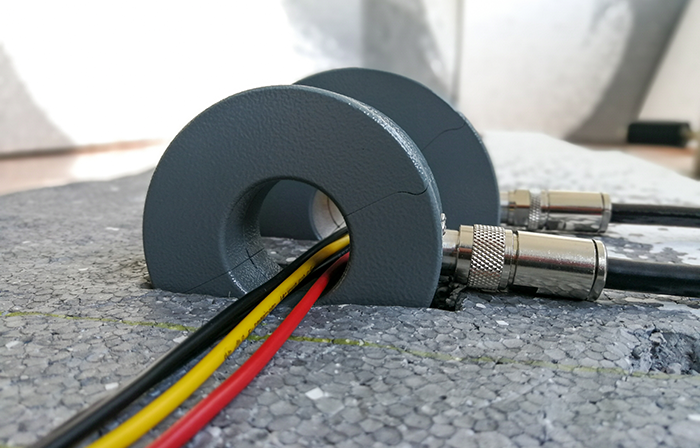
The test method is defined in ISO 11452-4, an international standard for automotive electromagnetic compatibility (EMC), and is a mandatory test for many automotive manufacturers. During the test, a clamp-type current probe called a BCI probe induces RF noise currents onto the cable. The standard test frequency range typically extends from 1 MHz to 400 MHz.
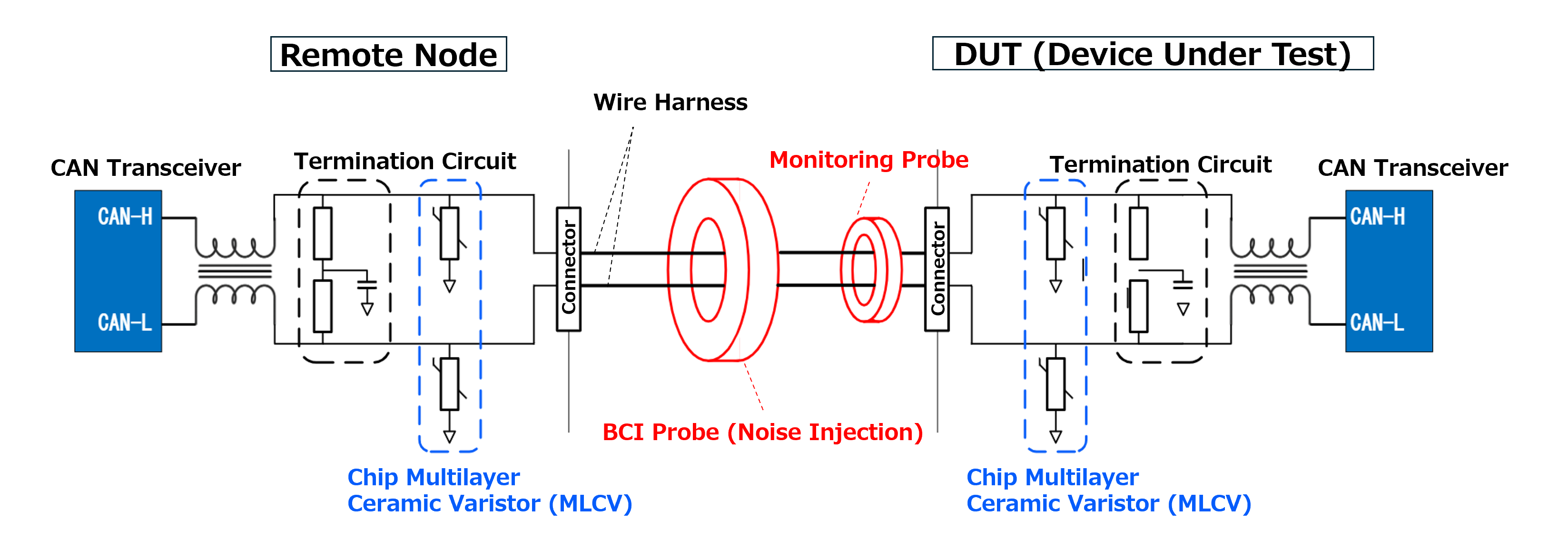
Evaluation is performed using either the substitution method or the closed-loop method. Noise currents are applied at various frequencies to achieve a specified current level (for example, several hundred milliamperes), and the impact on device operation is monitored. The objective is to ensure that automotive electronic systems can withstand RF noise originating from sources such as wireless communications and engine-related electromagnetic emissions encountered in real vehicle environments. Figure 1 shows the BCI test setup for a CAN-FD communication line.
2. Mechanisms Behind Communication Errors During BCI Testing
During BCI testing, high-frequency noise is injected into the wiring harness and appears as common-mode noise superimposed on communication lines, such as differential CAN-FD signal lines.
In an ideal differential transmission system, common-mode noise is canceled out. However, practical circuits contain slight asymmetries and nonlinear components that can convert common-mode noise into differential-mode noise—a phenomenon known as mode conversion. This occurs because impedance imbalances within the signal path and the nonlinear behavior of ESD protection devices can cause common-mode noise to appear as differential noise on the communication lines.
For example, ESD protection devices may exhibit diode-like rectification effects at high frequencies or experience sudden impedance fluctuations. As a result, common-mode noise is converted into differential noise that directly interferes with communication signals.
When noise affects the two differential lines unevenly due to circuit asymmetry, one line is affected slightly more than the other, causing the signal waveform balance to become distorted. Consequently, the differential voltage, which should remain constant, temporarily decreases. This can lead to bit decision errors at the receiving end and ultimately cause communication errors.
For example, in practical harness and transceiver designs, slight differences in signal line length, routing, and component characteristics are unavoidable, and the two lines therefore cannot transmit signals under perfectly identical conditions. During mass production, additional factors such as component variations among suppliers and differences in vehicle harness layouts must also be considered, as they can further contribute to waveform imbalance.
3. Examples of Communication Errors Caused by ESD Protection Devices
In automotive communication systems, protection devices such as TVS diodes and chip multilayer ceramic varistors (MLCVs) are commonly used for ESD protection. However, under certain conditions, these protection devices themselves can become a source of communication errors during BCI testing.
To evaluate the impact of ESD protection devices on communication quality, a comparison test was conducted on a high-speed CAN-FD bus operating at 5 Mbps. Three configurations were evaluated:
- A reference board with no ESD protection device
- A Panasonic chip MLCV (EZJPRV270RM, varistor voltage = 27 V, capacitance 15 pF)
- A competitor's TVS diode (VRWM = 24 V, capacitance = 6 pF)
During testing, RF current noise up to 200 mA was injected into an unshielded twisted pair (UTP) harness using a BCI probe over the frequency range of 1 MHz to 400 MHz. Communication errors were monitored throughout the test. Table 1 shows the results.
| Evaluation Sample | Test Results |
|---|---|
| Reference (No ESD Protection Device) |
PASS |
| MLCV (EZJPRV270RM, 2-in-1) |
PASS |
| TVS (2-in-1) |
Error (7 to 26 MHz) |
The comparison results revealed that neither the board without an ESD protection device nor the board equipped with the MLCV experienced communication errors at any tested frequency. In contrast, repeated communication errors were observed in the 7 MHz to 26 MHz range when the TVS diode was installed. These findings demonstrate that even if different ESD protection devices offer similar ESD protection performance, their noise susceptibility on high-speed CAN-FD lines can differ significantly across specific frequency bands, resulting in communication errors.
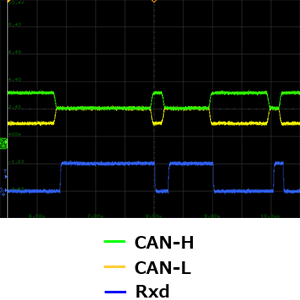
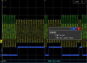
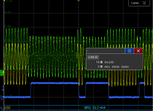
Figure 2 shows the CAN-H, CAN-L, and receiver output (Rxd) waveforms when a 10-MHz noise signal was injected during the BCI test. For both the reference board and the MLCV-equipped board, the CAN-H and CAN-L signals contained superimposed 10-MHz noise, yet the Rxd waveform remained unchanged from before BCI noise injection, indicating error-free communication. However, for the TVS-equipped board, the Rxd waveform deviated from its original pattern at the section in the red circle, demonstrating that data was no longer being transmitted correctly and that communication errors had occurred.
| Evaluation Sample | Before BCI Noise Injection | During BCI Noise Injection (10 MHz) |
|---|---|---|
| Reference (Without ESD Protection Device) |
 |
 |
| MLCV (EZJPRV270RM) |
 |
|
| TVS | 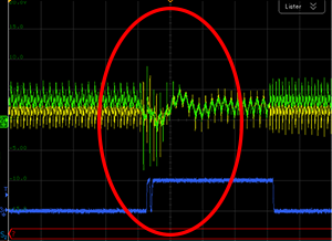 |
4. Mechanism of the Reverse Recovery Phenomenon in Zener Diodes
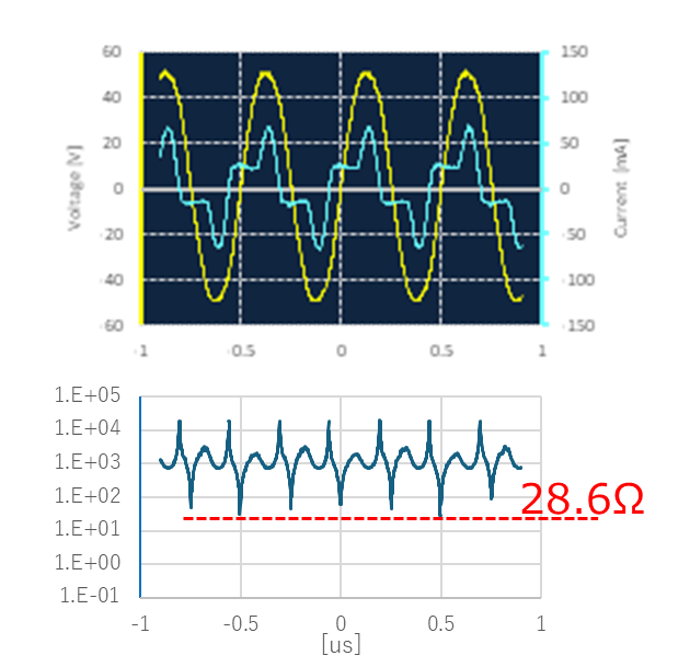
To investigate what was occurring in the Zener diodes (TVS), the electrical characteristics of the ESD protection devices were examined by applying a large-amplitude 2-MHz sinusoidal noise signal directly to each device.
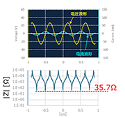
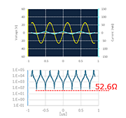
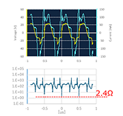
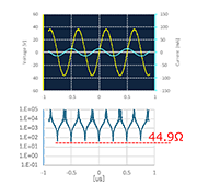
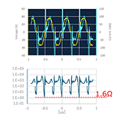
The analysis revealed that the waveform distortion exhibited by the Zener diode originated from a phenomenon unique to PN diode devices known as reverse recovery. Specifically, when the polarity of the applied sinusoidal signal reverses while the diode is conducting a sufficiently large forward current, the charge stored within the diode rapidly discharges, resulting in a large reverse current flow.
This reverse recovery current causes the impedance between the diode terminals to drop dramatically—sometimes to only a few ohms—for a brief period (Figure 3). During the evaluation, the MLCV maintained an impedance of approximately 30 Ω even while operating. In contrast, the impedance of the Zener diode decreased to approximately 1 to 2.5 Ω at the moment of polarity reversal.
As a result, the apparent impedance between the CAN-FD communication line and ground becomes significantly lower than the 60 Ω termination resistance. Consequently, the communication signal can no longer maintain its normal amplitude, ultimately leading to communication errors.
| Applied Voltage | MLCV EZJP0V270RM |
TVS (Supplier A) |
TVS (Supplier B) |
|---|---|---|---|
| Approx. ±27 Vpp |
 |
 |
 |
| Approx. ±37 Vpp |
 |
 |
 |
| Approx. ±54 Vpp |
 |
|
|
5. Differences Between Zener Diodes and MLCVs Based on V-I Characteristics
The differences in behavior between Zener diodes (TVS) and MLCVs can also be understood by examining their static voltage-current (V-I) characteristics.
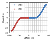
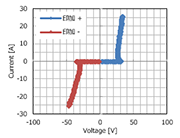
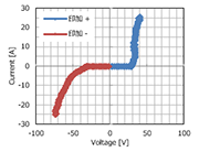
Measurements performed using the Transmission Line Pulse (TLP) method showed that the Zener diode exhibited polarity-dependent behavior. Its operating voltage and current rise characteristics differed between positive and negative polarities, resulting in an asymmetric V-I characteristic (Figure 4).
Even devices marketed as “bidirectional TVS diodes” do not always exhibit perfectly symmetrical V-I characteristics in practice. Differences between the positive and negative operating polarities can cause conduction to occur earlier in one direction than in the other. Consequently, one side of the waveform may be preferentially clipped, producing a rectification-like effect that can amplify the influence of high-frequency noise.
By contrast, the MLCV exhibited a nearly symmetrical V-I curve for both positive and negative polarities. Because of its inherently symmetrical structure and the absence of charge-storage delay, the MLCV demonstrated stable behavior under high-frequency noise conditions during this evaluation and did not generate communication errors.
In other words, the operating characteristics of ESD protection devices under high-frequency noise conditions vary significantly depending on device type. These differences can directly affect signal waveform integrity by introducing distortion and amplitude fluctuations, ultimately influencing the stability and reliability of communication systems.
| MLCV/Panasonic EZJP0V270RM |
TVS (Supplier A) |
TVS (Supplier B) |
|
|---|---|---|---|
| Operating Voltage | 27 V typ. @1 mA | 30 V typ. @10 mA | 27 V @1 mA |
| Capacitance | 15 pF typ. @1 MHz | 5.2 pF @1 MHz, DC 2.5 V | 30 pF typ. @1 MHz |
| Polarity | Bidirectional | Bidirectional | Bidirectional |
| ■ Comparison of Voltage-Current Characteristics | |||
| Voltage-Current Characteristics (TLP) |
 |
 |
 |
| Polarity | Bidirectional | Bidirectional | Bidirectional |
| Symmetry | Symmetric | Asymmetric | Asymmetric |
| Nonlinearity | △ | 〇 Kickback Observed |
△ Positive/Negative Characteristics Vary |
6. Key Considerations for Selecting and Designing ESD Protection Devices
The findings discussed above demonstrate that appropriate ESD protection device selection and circuit design are critical for preventing communication errors in high-frequency noise environments such as those encountered during BCI testing. The following three points should be carefully considered when selecting ESD protection devices for automotive communication lines.
Sufficiently High Operating Voltage
The protection device should be selected so that it does not unintentionally enter conduction in response to normal communication signals combined with external noise. The Zener voltage or varistor voltage should exceed the maximum expected signal-plus-noise level. Ideally, the voltage margin should be large enough to prevent the protection device from operating under the sinusoidal noise conditions typically encountered during BCI testing.
Symmetrical Characteristics for Both Polarities
For differential communication lines, it is desirable to use protection devices that exhibit symmetrical operating voltages for both positive and negative polarities. In the case of Zener-based devices, the post-breakdown V-I characteristics—including dynamic resistance and current behavior—should be as balanced as possible in both directions. Greater symmetry reduces the likelihood that common-mode noise will be converted into differential-mode noise.
Excellent Reverse Recovery Performance (Trr)
When employing Zener diodes (TVS), devices with short reverse recovery times (Trr) and minimal device-to-device variation should be selected. Reducing reverse recovery current helps suppress the temporary impedance drop discussed earlier, thereby minimizing its impact on communication signal integrity.
7. Features of Automotive CAN-FD-Compatible 2-in-1 Chip Multilayer Ceramic Varistors
As demonstrated in the previous sections, communication errors during BCI testing are strongly influenced by the operating characteristics of the ESD protection device itself. One technology that has attracted attention as an effective alternative to Zener diodes (TVS), which may induce communication errors, is the chip multilayer ceramic varistor (MLCV).
MLCVs utilize a multilayer ceramic dielectric structure and do not employ PN junctions. As a result, they are inherently less susceptible to reverse recovery current generation, helping the device impedance to remain relatively stable during high-frequency noise injection and suppressing signal waveform distortion.
Another key feature of MLCVs is their nearly symmetrical V-I behavior for both positive and negative polarities. This symmetry reduces the likelihood of common-mode noise being converted into differential-mode noise on differential communication lines, helping maintain waveform integrity (Figure 5).
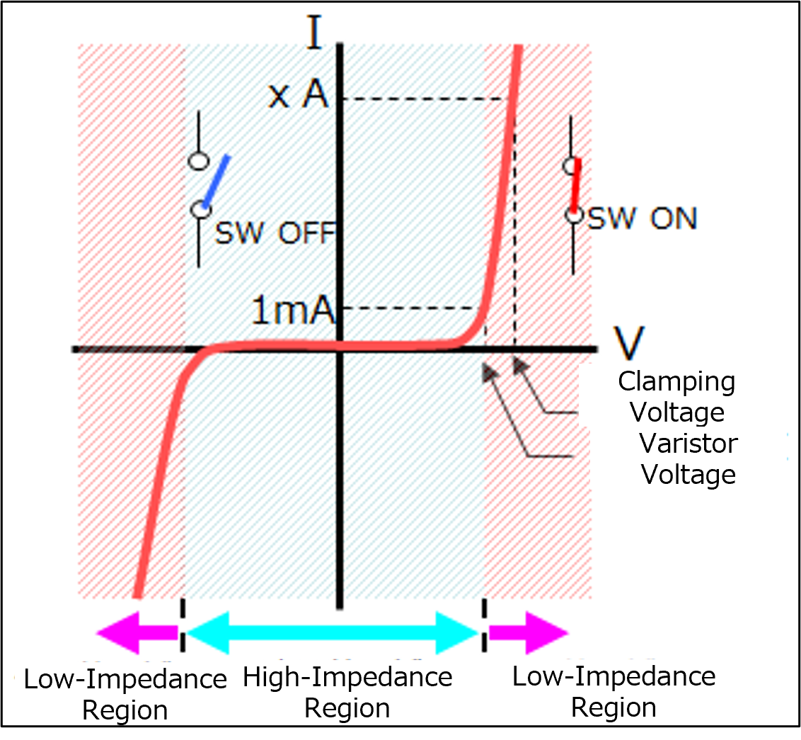
This advantage becomes particularly important in high-speed differential communication systems such as CAN-FD and Automotive Ethernet, where even slight waveform distortion can affect signal rise times and amplitudes, potentially leading to incorrect bit detection. By minimizing these effects, MLCVs contribute to more robust and reliable communication.
Recently, 2-in-1 MLCVs specifically designed for CAN-FD differential-pair protection have become available. The device evaluated in this study is one such example. In a 2-in-1 configuration, two varistor elements are integrated into a single package, providing dedicated protection for both CAN_H and CAN_L lines.
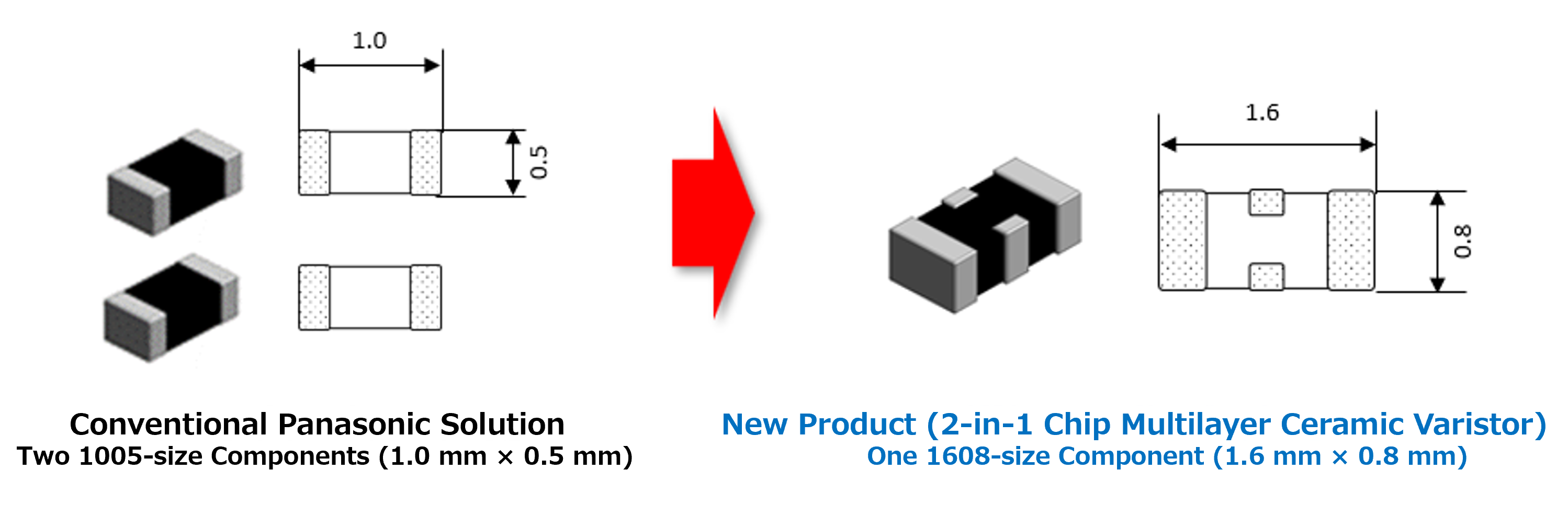
Because both protection elements are fabricated on the same chip, variations in electrical characteristics are minimized. Consequently, both communication lines receive virtually identical protection behavior. This helps prevent situations where one signal line experiences excessive clamping compared to the other, thereby maintaining differential signal symmetry.
In addition, capacitance mismatch between the two protection elements is small. This minimizes mode conversion caused by capacitance imbalance and is expected to reduce communication errors during BCI testing.
The 2-in-1 MLCV combines the essential protection performance required of an ESD protection device with a low tendency to generate reverse recovery current while simultaneously suppressing mode conversion effects. For these reasons, it is expected to become an attractive solution for next-generation automotive communication designs.
8. Summary
Cases have been reported in which high-frequency noise applied during BCI testing distorts communication waveforms and causes communication errors. One possible cause is that ESD protection devices respond to noise current, resulting in a temporary reduction in impedance and instability in signal transmission.
In particular, Zener diodes (TVS) may experience reverse recovery current when the voltage polarity reverses. During this brief interval, the impedance across the device can drop to only a few ohms. Consequently, communication signal current is diverted toward ground, reducing differential voltage levels and potentially causing bit decision errors.
By contrast, chip multilayer ceramic varistors (MLCVs) do not contain PN junctions and are therefore much less likely to generate reverse recovery current. Even during operation, they can maintain impedance at the level of several tens of ohms. Furthermore, they exhibit nearly symmetrical V-I characteristics for both positive and negative polarities.
As a result, common-mode noise is less likely to be converted into differential-mode noise and waveform distortion can be minimized, preventing communication errors even under BCI test conditions.
These characteristics allow MLCVs to provide both effective ESD protection and stable communication performance in electrically noisy environments. As high-speed automotive communication technologies such as CAN-FD and Automotive Ethernet become more widespread, MLCVs are expected to play an increasingly important role as a key solution.
9. Related Product Information
10. Related Articles
- On-board CAN-FD compatible "Chip Type Multilayer Varistor 2-in-1 Type"
- Basics of Electrostatic Discharge (ESD) Suppression and Testing Processes
- Points for Selecting ESD Suppression Circuits and Components for Automotive Electronic Devices
- Basics of Surge/ESD and Protection Components
- Noise-reducing measures start with knowing about the different types and properties of noise.
11. Tags Related to This Article
 Search by
 Search by
 Search by