Basics of Surge/ESD and Protection Components - Panasonic
2017-11-07
What is Surge and ESD?
Surge and ESD (electro-static discharge) refer to transient high voltage, and possibly a very dangerous noise under certain conditions. A Surge and ESD may cause malfunctions to the equipment or circuit when the level reaches a certain degree, and the level often experiences high voltage far exceeding the permissible range. In such cases, the affected component or equipment is broken in an instant. The diagram is a mapped image of surge voltage and its width.
Surge and ESD are described below.
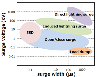
① Lightning surge
Lightning as natural phenomenon contains a very large amount of energy. A lightning surge can be grouped into direct lightning surges and induced lightning surges. Protection against a direct lightning surge is difficult, but protection against induced lightning is possible. Induced lightning is a high voltage surge induced by a relatively long wire such as power line or communication cable that is nearby a lightning strike. It is presumed that the generation mechanism is an electric charge induced in a cable that is in proximity of an electric field discharged by a lightning strike, or a magnetic field generated by a lightning strike current generates an inductive electromotive force in the cable. As shown in the previous diagram, an induced lightning surge has a large amount of energy that can easily destroy electric or electronic components even though it is not as destructive as a direct lightning surge, thus requiring prevention measures.
② Open/close surge
Open/close surge is a transient high voltage surge induced in a switch or relay during its on and off operation, particularly when turning off, which causes rapid current change and inductance of the circuit or wiring. Voltage generated by an open/close surge is very high, and in some cases, it generates spark, heat or radiates an electromagnetic wave caused by a large damping oscillation current generated by parasitic capacitance of inductance and contact. This high voltage surge may cause a malfunction of an electronic circuit, and in some cases, lead to the destruction of a component. And the emission of an electromagnetic wave through damping oscillation causes EMI, thus requiring suppression measures for an open/close surge.
③ Load dump
Load dump is a surge generated by cutting the battery connection off on an automobile. The most severe instance occurs when the battery connection is lost while the automotive engine is in operation and the alternator (battery charging generator) is charging the battery. The magnitude of surge voltage is determined by the alternator rotation speed and magnetic field excitation strength at the moment of cut off. Surge voltage exceeds 100 V in some cases for a duration of several hundred milliseconds. Because this surge has such a large amount of energy, it can easily destroy an electronic component. Permissible load dump is specified by auto-makers and automotive equipment makers in the form of maximum voltage, line impedance, and duration time. For load dump testing, JASO A-1 (Japan) and ISO-7637-2 Pulse 5 (U.S.) is applied.
④ ESD
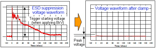
ESD (electrostatic discharge) is a phenomenon where a charge is stored in a small floating capacity on a human body or substance then discharged to a nearby object, and is classified as one type of surge. ESD duration time is short with little energy, but because it generates transient high voltage as high as several kilo volts, it can generate a malfunction of electronic circuits or damages electronic components.
For the evaluation and testing method of an ESD, a human model or machine model is generally used. And protection is possible by utilizing the components based on these assumptions.
Surge/ESD Protection Components
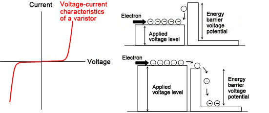
For the purpose of protection against a surge and ESD, use of a varistor or zener diode is the general choice. These components have a high electrical resistance when the terminal voltage is low, but the resistance suddenly becomes low when the voltage gets higher.
By using this tendency, the component prevents a surge from entering the circuit by bypassing the current when a high voltage surge occurs in an electric circuit.
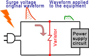
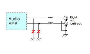
The diagram to the right illustrates how to protect a power supply circuit from induced lightning surge by using a varistor. By connecting a varistor in parallel with the power input side line, an induced lightning surge, as high as several-thousand volts, is restricted by the varistor to a level that won’t cause component destruction or deterioration of the power supply circuit.
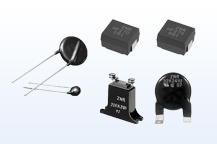
Actual surge/ESD protection components, those optimized for surge type and line (signal, power, etc.) that need to be protected are available.
Among those components, we selected the “ZNR®” surge absorber, chip varistor, and ESD suppressor were selected.
“ZNR®” surge absorber is a Panasonic product name, the varistors are designed for protection against surges.
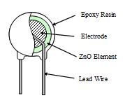
“ZNR®”surge absorber
Panasonic“ZNR®”surge absorber is a ceramic varistor for surge absorption against induced lightning surge, open/close surge and load dump surge.
Panasonic was the first manufacturer in the world that commercialized ceramic varistors with a superior ceramic material design and process technology backed by many achievements in device design and production engineering. “ZNR®”surge absorbers are produced mainly from the material zinc oxide (ZnO) and several additives, as well as the ceramic element created using the sintering technique. This product provides excellent voltage non-linearity characteristics in parallel with those of zener diodes along with large current resistance characteristics not found in other products. This product can be used for a wide variety of applications such as voltage stabilization, pulse voltage suppression, open/close surge voltage absorption, and protection from a lightning surge.
“ZNR®”is an acronym of Zinc-oxide Non-linear Resistor, and is a registered trademark of Panasonic.
Principal Specifications of the “ZNR®” Surge Absorber
Principal specifications of the “ZNR®” surge absorber are shown indicating performance.
| Spec Items | Description |
|---|---|
| Varistor Voltage [V] | In principle, voltage value at both ends of a component when DC 1 mA is applied. This is the guideline value of voltage when varistor operates. |
| Maximum allowable circuit voltage [V] | Maximum value of the commercial frequency sinusoidal wave voltage effective value allowing continuous application, or maximum value of DC voltage. |
| Maximum restricted voltage [V] | When a surge voltage is applied, the voltage value restricted by the varistor is called restricted voltage, and an individual catalog lists the maximum restricted voltage as maximum value. |
| Surge current resistance [A] | This value indicates the level of surge current resisted by the varistor. |
| Safety Standard | For components subject to a lightning surge, each country specifies safety standards such as UL (USA), CSA (Canada), IEC (Europe), CQC (China), and the components meeting the standards must be used in that country. |
Whether the specification meets the presumed surge voltage/current and circuit voltage used is examined when selecting a “ZNR®” surge absorber.
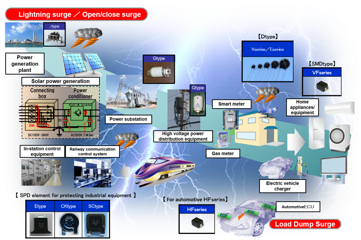
Example of Using a “ZNR®” Surge Absorber
The “ZNR®” surge absorber has a broad lineup that supports power plants and general electronic devices.
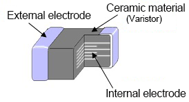
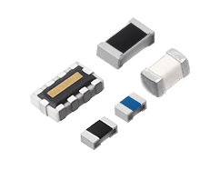
Chip Varistors
Chip varistor is a chip-shaped laminated varistor, and the basic structure is a laminated ceramic component similar to a laminated ceramic capacitor (MLCC). As explained above, the “ZNR®” surge absorber is ceramic varistor, a chip varistor belongs to the same group. However, the voltage and current handled by a chip varistor are substantially smaller than that of a “ZNR®” surge absorber, and used primarily for protection against ESD.
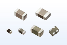
- Panasonic chip varistor has the following features.
-
- Small surface-mounted type (0603, 1005, 1608) enables compact sizing and light weight for a wide variety of application.
- Unique ceramic material and process technology provide high reliability, high ESD suppression effect, high ESD resistance, and high surge resistance.
- Lineup of automotive grade components (ISO/TS16949 certified)
- Long-term life warranty (Loaded life 2000 hours, temperature cycle 2000 cycles, high thermal resistance (150℃)
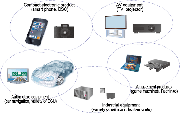
Examples of Using Chip Varistors
Chip varistors are used in a wide variety of electronic equipment as general purpose ESD protection components.
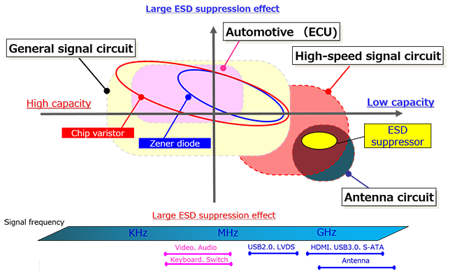
ESD Suppressors
ESD suppressor is a gapped type ESD (electro-static discharge) protection component. The minimized static capacitance is suited for using in a high-speed signal line.

Compared with the chip varistors described above, an ESD suppressor has a very small electrostatic capacitance and is a major difference in characteristics. The voltage-current characteristics can accommodate an ESD in the range of several kilo-volts. A very small electrostatic capacitance 0.05 pF or below (0603, 1005 size) causes almost no impact on transmission characteristics of a high-speed differential signal circuit or on insertion loss in a high-frequency circuit.
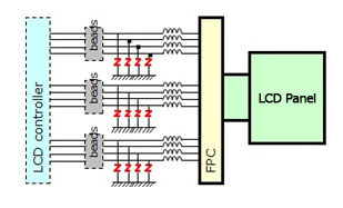
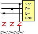
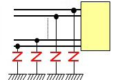
Examples of Using ESD Suppressors
- Shown below are the examples of using ESD suppressors.
-
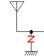
- Antenna circuit (GPS, NFC, etc.) of a mobile electronic product
- Antenna circuit of automotive equipment (car navigation, AM/FM, automotive AV system)
- High-speed differential signal circuit (USB2.0/3.0、HDMI1.4/2.0)
- Variety of signal lines
differential
transmission
Advantage of replacing the zener diode
As an anti-surge/ESD component, a zener diode can be used instead of a varistor or ESD suppressor. The advantage of replacing a zener diode with a varistor (“ZNR®” surge absorber, chip varistor) is described here.
What is a zener diode?
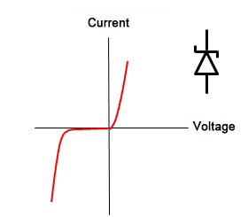
Before replacement, we should know what a zener diode is first.
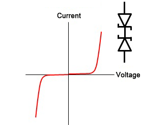
The voltage and current characteristics of a zener diode are shown below. A single zener diode provides voltage restriction effect only at the negative voltage side, but by using two diodes in an opposite series connection, bidirectional voltage restriction effect can be obtained, as is the case in a varistor.
For an advantage over a varistor, effective protection voltage can be set at a low level of several volts.
of a zener diode (single unit)
of zener diodes (2 units connected)
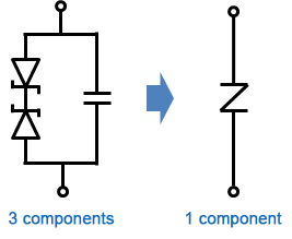
However, for disadvantage, they require a large shape and more weight as well as a larger mounting surface area than a varistor. In order to obtain the same surge/ESD absorbing effect as a varistor, the unit needs to be constructed with 3 components, including a capacitor, instead of a single varistor.
Although a bidirectional zener diode is available by connecting two diodes in a single package, it is still larger than the size of a varistor.
Advantages of replacement by a varistor
When zener diodes are replaced with a varistor (“ZNR®” surge absorber, chip varistor), the following advantages can be obtained.
Advantage 1: Compact-sizing, lightweight, and mount area reduction
As described, surge protection by using zener diodes requires 3 components, but a single varistor can serve the same function, thereby achieving a substantial reduction of size, weight and mounting surface.
In the case of automotive load dump prevention, replacing 5 W zener diodes with a “ZNR®” surge absorber (SMD type HF series) can reduce both mounting surface and weight by 67%.
In the case of ESD prevention, replacing 0.2 W zener diodes with a chip varistor (1005 size) can reduce the mounting surface by 85% and weight by 75%.
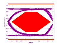
Advantage 2: Improved resistance to ESD and surge current
The graph shown below is a comparison of resistance to ESD and surge current between 0.2 W zener diodes and a chip varistor (1005 size) as described above.
The graph shows that resistance to ESD and surge current improves by replacement with a chip varistor.
0.2W ZD
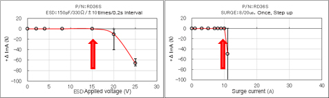
ESD:15kV Surge:10A
1005 Chip Varistors
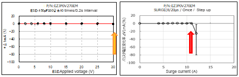
ESD:30kV Surge:11A
Summary of ESD Prevention Components
As ESD prevention components, we reviewed the chip varistor, ESD suppressor, and zener diode. The difference and features of each component are summarized in the table below.
| Zener diode | Chip Varistors | ESD Suppressors | ||
|---|---|---|---|---|
| Features |
|
|
|
|
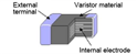
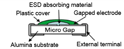
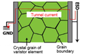
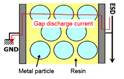
| Material | Si semiconductor | Compound semiconductor | Polymer compound | |
| Structure | 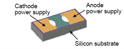 |
 |
 |
|
| Discharge mechanism | 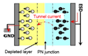 |
 |
 |
|
| Electrical characteristics | ||||
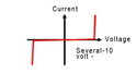
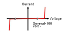
| Protection operation voltage | Several volt - | Several-10 volt - | Several-100 volt - | |
| Electrostatic capacitance | 0.3pF - | 10pF - Several-100 pF |
0.05pF | |
| Voltage-current characteristics |  |
 |
 |
|
Application coverage for each ESD prevention component is summarized in the diagram below.
Related product information
Tags related to this article
This document summarizes the Noise measures related articles posted as technical information for the Optimal Solutions for Circuit Design.