Basic Knowledge of Power Circuits (2)
-Operation of the Switching Regulator-
2019-07-22
In the previous section on the Basic Knowledge of Power Circuits (1), we classified power circuits by paying attention to input/output voltages. This section focuses on the switching regulator, which is the most commonly used power circuit among those power circuits. By using the step-down switching regulator as an example, we will further discuss the circuit configuration and operational mechanism of the switching regulator in detail.
Features of the switching regulator
The switching regulator is incorporated into many pieces of equipment and devices, such as smartphones, computers and their peripheral equipment, digital household appliances, and cars (electronic control units or ECU). The switching regulator is a sort of DC/DC converter that converts a DC voltage into another DC voltage. The switching regulator has the following features.
- The switching regulator can make up a step-down power circuit (input voltage > output voltage), a boost power circuit (input voltage < output voltage), and a step-up/step-down power circuit.
- The switching regulator generally has high energy conversion efficiency ranging from 80% to 90%, thus causing less (heat) power loss at the power circuit.
- It also allows production of a low voltage output of 1.0 V or lower (sub-volt), which microprocessors and AI processors have needed in recent years, and a large current output of 100 A or larger.
- The switching regulator provides a rich lineup of commercially sold solutions, such as controller ICs and switching regulator modules.
Basic configuration of the step-down switching regulator
A basic circuit of the step-down switching regulator circuit is composed mainly of the following elements.
- Input capacitor Cin
Input capacitor Cin absorbs fluctuations in an input current. Its capacitance generally ranges from several tens of μF to several hundreds of μF. To achieve higher response, the input capacitor Cin may be made up of low-capacitance capacitors connected in parallel.
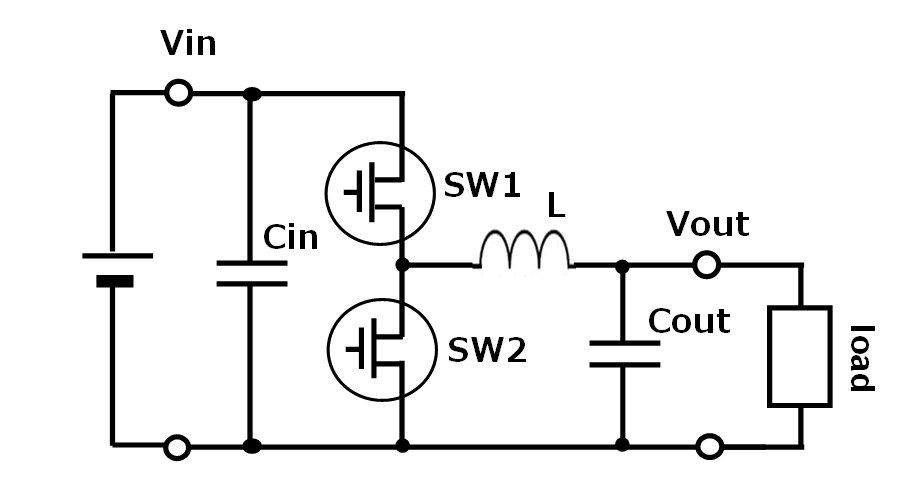
- Switch element SW1
As indicated by the name of the switching regulator, switch element SW1 performs switching operations, and it is sometimes called a high-side switch. In general, a MOSFET is used for the switch element. - Switch element SW2
Switch element SW2 is an element that, by its switching operations, forms a loop between output inductor L and a load. It is also called a low-side switch. Although a diode used to be used for SW2, a control method using a MOSFET for SW2 (synchronous rectifying method) has become popular these days to meet the demand for higher energy conversion efficiency. - Output inductor L
Output inductor L saves energy when switch element SW1 is on, while releasing energy when switch element SW1 is off. The inductance of output inductor L generally ranges from several nH to several μH. - Output capacitor Cout
Output capacitor Cout absorbs fluctuations in output voltage caused by the switching operations, thus smoothing out the output voltage. The output capacitor Cout has a capacitance generally ranging from several μF to several tens of μF. To achieve a higher response, the output capacitor Cout may be made up of low-capacitance capacitors connected in parallel.
Outline of the operation of the step-down switching regulator
We will now outline the operation of the step-down switching regulator.
Switching between two modes
Roughly speaking, the switching regulator operates in two modes.
In one mode, switch element SW1 is on while switch element SW2 is off. In this mode, the equivalent circuit of the circuit in Fig. 1 is depicted as the circuit in Fig. 2(a) in which energy is accumulated at output inductor L.
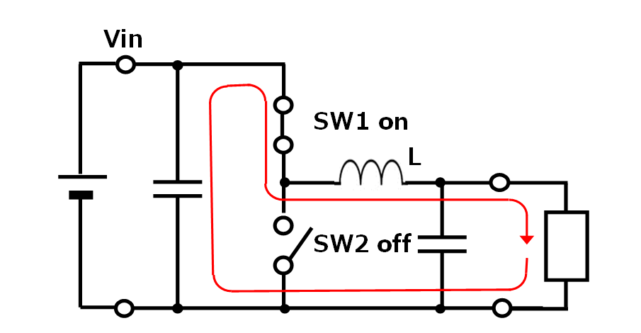
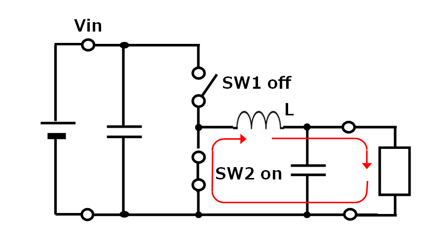
The switching regulator repeats these two modes by turning cyclically, thus turning the input voltage Vin into a given voltage. Meanwhile, under the influence of the switching on/off of switch element SW1, a current flowing through inductor L takes a serrated shape shown in Fig. 3. The output voltage Vout, on the other hand, basically remains constant because it is smoothed out by the output capacitor Cout (strictly speaking, however, the output voltage Vout fluctuates slightly).
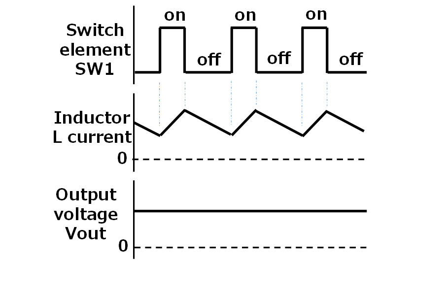
on/off of the switch element SW1 and
a current flowing through the inductor L
The output voltage Vout is determined by a ratio between the on-period of the switch element SW1 and the off-period of the same. If we assume that other circuit elements suffer no loss caused by their resistive components, we can calculate the output voltage Vout using the following equation.
On period
On period + Off period
A term "on-period / on-period + off-period" included in the equation is called duty cycle or duty ratio. For example, in a case where the output voltage Vout of 6 V results for the input voltage Vin of 12 V, the duty cycle is calculated at 6 ÷ 12 = 0.5. This means that switch element SW1 needs to be switched on in a period that is 50% of its entire operation period.
Controlling the output voltage based on its ratio to a reference voltage
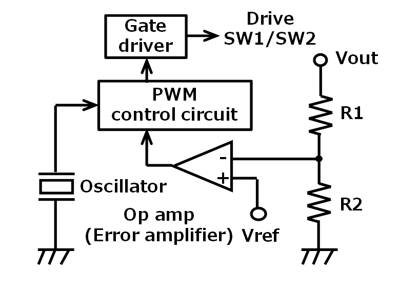
making up the switching regulator
These circuit elements work in the following manner.
The amplifier compares output voltage Vout with reference voltage Vref, and sends the result to the PWM control circuit. When output voltage Vout is lower than reference voltage Vref, the on-period of switch element SW1 is increased to raise output voltage Vout. When output voltage Vout is higher than reference voltage Vref, in contrast, the on-period of switch element SW2 is reduced to lower output voltage Vout. In this manner, output voltage Vout is maintained constant.
Now, let's take a closer look at the amplifier, oscillator, and gate drivers shown in Fig. 4.
-
- Amplifier (error amplifier)
- The amplifier, because of its function of detecting a difference between reference voltage Vref and output voltage Vout, is called an "error amplifier." Since reference voltage Vref remains constant, the ratio between resistance R1 and resistance R2, which make up a voltage divider circuit, determines output voltage Vout. When reference voltage Vref is maintained constant, therefore, the following equation holds.
-
Vref = Vout ×
R2
R1 + R2
⇒Vout
Vref
=R1 + R2
R2
- For example, if you want to obtain output voltage Vout = 6 V by giving the switching regulator reference voltage Vref = 0.6 V, you need to determine the values of resistances R1 and R2 such that (R1 + R2)/R2 = 10 holds.
The reference voltage Vref may be created by a method utilizing a forward voltage drop (about 0.6 V) generated across the pn junction of a diode. This method, however, involves a thermal coefficient (kT/q), which makes the method slightly inaccurate. To set the reference voltage Vref more accurately, it is better to use a reference voltage-generating circuit with a temperature compensation function.
-
- Oscillator circuit
- The oscillator outputs a signal with a given frequency necessary for the switching operations. The switching frequency generally ranges from several tens of kHz to several MHz. When the switching regulator is incorporated into car equipment, for example, the switching frequency is set to 2 MHz or so to prevent its interference with the radio frequency. In many cases, a voltage control oscillator is employed to set a switching frequency optimal for a given system in a flexible manner.
-
- Gate driver
- The gate drivers drive SW1 and SW2. When MOSFETs are used for the switch elements, switching them on and off requires drivers capable of sufficiently charging the input capacitance of the gates of the MOSFETs. In particular, a large MOSFET capable of driving a large current has a large gate capacitance, so that actuating the MOSFET requires a driver that supplies a current sizable enough to meet the large gate capacitance. For this reason, the gate driver circuit needs to be tailored to selected MOSFETs.
Challenges for switching regulators
As mentioned above at the start of this section, the switching regulator offers various advantages. However, it also has some problems that need to be addressed.
Unstable operation
The error amplifier shown in Fig. 4 forms a feedback loop for adjusting the output voltage Vout. It should be noted, however, improperly designing the feedback loop causes the whole circuit to operate unstably or oscillate. To ensure stable circuit operation, properly determining a feedback loop band and a phase margin is essential, but rather troublesome.
Usually, however, you will not have a problem if you assemble the circuit using a commercially sold control IC and refer to data listed in the datasheet.
Electromagnetic noise generation
As depicted in Figs. 2(a) and 2(b), the current flowing through the power circuit changes greatly depending on whether switch element SW1 is on or off. A current loop creates a magnetic field, and a change in the current results in a change in the magnetic field's intensity. Because of this principle, electromagnetic noise is generated in synchronization with the switching cycle. This electromagnetic noise may affect other circuits if it is not suppressed by a proper anti-noise measure.
In the next section, we will discuss switching power supply design, focusing on the electromagnetic noise problem and measures against it.
Tags related to this article

This document summarizes the Basic knowledge of power supply circuit posted as technical information for the Optimal Solutions for Circuit Design.