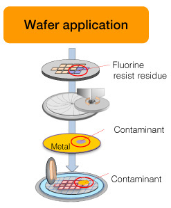
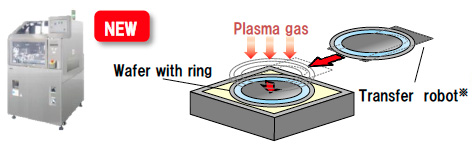
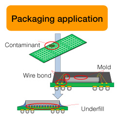
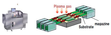
Plasma Cleaning Process
PSX307A
- Wafer cleaning/modificationfor flip chip die attach/solder ball attach/stack die attach
- Solder ball cleaning for WLCSP
- De-scum process for plating process
PSX307
- Electrode cleaning for wire bonding& flip-chip bonding
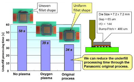
- Surface modification for mold and underfill
Plasma Cleaning Process Application
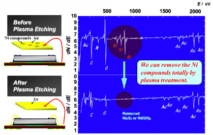
Wire-BondingBondability
Memory
UnderfillAdhesive
Processor
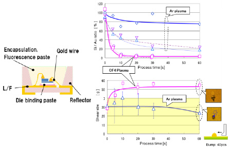
LED PackingBondability
LED
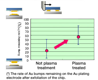
Flip-Chip BondingBondability
SAW
RF module
Feature of Plasma Cleaner PSX Series
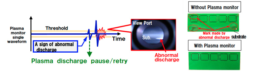
Plasma monitor allows to avoid abnormal discharge on thin substrate
Panasonic Patent
- Prevent defect substrate passing to next process.
- Record the log data of monitor for each substrates(option).
Process analysis & solution proposal for customer
- Provide issue-solving consulting for customer.
- Implement demonstration with analytical equipment and support process improvement.