Your Value
- Downsizing
- Cost Reduction
- High Performance
| Solution for Value Realization | Model | ||
|---|---|---|---|
| MD-P200 | MD-P200US2 | MD-P300 | |
|
(1) High Accuracy Multi Die Bonding
|
○ | - | - |
|
(2) Stacked Die Bonding
|
○ | - | - |
|
(3) Flip Chip Bonding
|
○ | ○ | ○ |
| Products | Package |
|---|---|
| Smartphone • PC • Wearable Device • Automotive • loT Device etc. | Processor • Communication Device/Module • Camera Module • LED • Power Device • MEMS • Sensor etc. |
(1) High accuracy multi die bonding
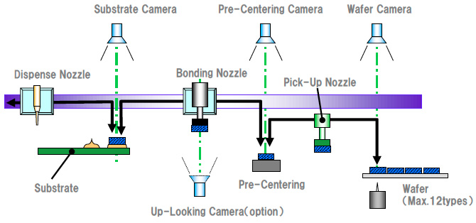
Epoxy dispensing before bonding : MD-P200
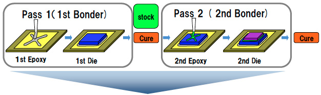
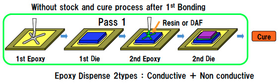
(2) Stacked Die Bonding by one bonder
Competitor
Panasonic : MD-P200
(3) Flip Chip Bonding
Example (process : C4/US)
Example : CSP Packaging Process
Process:C4

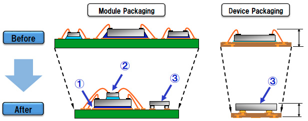
Example : Compact Device Packaging Process
