Solutions for LED &Power Device by Dry Etching
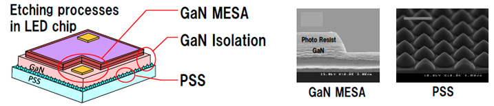
LED
• APX300 contributes to high productivity of GaN etching by low damage and high rate processing
• APX300 contributes to high brightness by PSS processing
• Available for 2, 4, 6 inch multi wafer processing
(PSS=Patterned Sapphire Substrate)
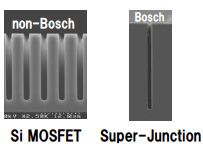
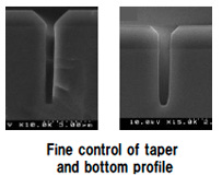
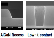
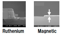
Power Device (Si, SiC, GaN)
• Panasonic realizes high performance etching for next gen. power devices
| Si Power Devise | SiC Power Device | GaN Power Device | Related Process |
|---|---|---|---|
 |
 |
 |
 |
Solutions for Communication Device& MEMS・Sensor
SAW Device / High speed Communication Device
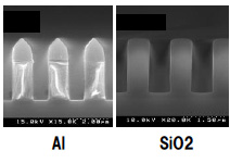
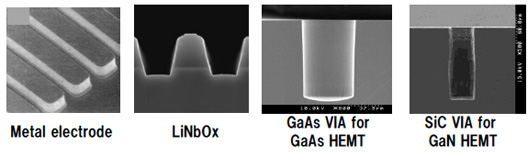
• IDT(Inter Digital Transducer)& various metal fine processing
• Thick SiO2 layer & LT/LN etching, APX300 realizes to high productivity by multi-wafer processing
• High rate deep etching of compound semiconductor substrate by high density plasma source
• GaAs scribe & dicing available
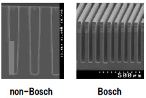
MEMS (Piezoelectric, Non-volatile materials, Si)
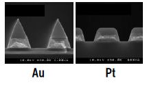
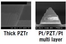
• Etching of Various materials(Piezo, Non-volatile, Si) such as the gyro, pressure sensors and printer head
| Au・Pt electrode | Piezoelectric | Non-volatile | Si |
|---|---|---|---|
 |
 |
 |
 |