2020-06-15
Problem solving example
Technical information
ESD Controls for Automotive LAN (Ethernet)
Introduction
Communication networks of the ECU (electronic control unit) of automotive systems use standards such as CAN and LIN. Among these standards, the automotive Ethernet, which is a high-speed communication standard of 100 Mbps or higher, is considered promising for achieving ADAS (advanced driver-assistance systems), which has been attracting attention in recent years. As with other standards, protection against ESD is absolutely essential. Although automotive Ethernet PHY (physical layer IC) vendors recommend ESD control methods, there are several issues with them. A control method using high withstanding type ESD suppressors will be proposed here as a more effective method of ESD control for automotive Ethernet.
ESD Controls Recommended by Automotive Ethernet PHY Vendors and their Issues
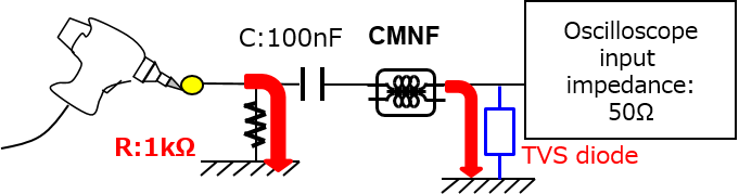
As in the case of CAN, the principle approach of ESD controls for networks usually involves placing ESD control components directly below a connector serving as a connection point between equipment and units and a network (cable). On the other hand, automotive Ethernet PHY vendors recommend a configuration in which TVS diodes, which are ESD control components, are placed between CMNFs (common mode noise filters) and PHY. This is because configurations with TVS diodes placed directly below the connector in the case of automotive Ethernet cause communication errors in the Bulk Current Injection (BCI) Test, which is adopted by a number of automobile-related manufacturers (details to be provided later).
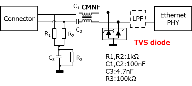
The TVS diodes are placed between the CMNFs and PHY instead of directly below the connector.
However, this circuit configuration, in which TVS diodes, i.e., ESD control components, cannot be placed directly below the connector, will have two issues.
- Decline in ESD protection effects for PHY (physical layer IC)
- Degradation of terminal resistances R1 and R2 due to ESD
ESD Control Circuit that Solves these Issues by Using High Withstanding Type ESD Suppressors
As recommended by automotive Ethernet PHY vendors, an ESD control circuit that uses high withstanding type ESD suppressors instead of TVS diodes to solve the two issues with the ESD control circuit is shown below.
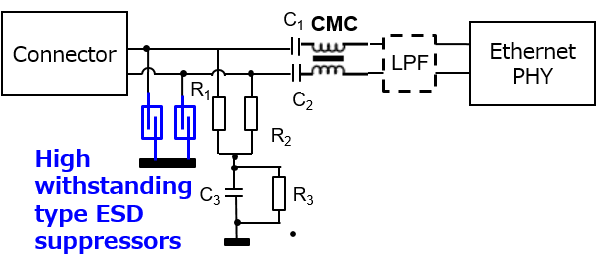
High withstanding type ESD suppressors can be placed directly below the connector.
Using high withstanding type ESD suppressors instead of TVS diodes enables the placement of ESD control components directly below the connector.
Verification by BCI Test
The BCI (Bulk Current Injection) Test, which evaluates malfunction levels and interference elimination capabilities by injecting RF current into the power and signal lines of automotive electric and electronic components using a BCI probe, has been adopted by a number of automobile-related manufacturers. The effectiveness of each ESD control circuit configuration was verified with this BCI Test.
During the test of the circuit (ESD_1) using the principle approach, i.e., ESD control components being placed directly below the connector, communication errors occurred in the case of TVS diodes, whereas there were none with high withstanding type ESD suppressors (see the table). This result confirmed that automotive Ethernet PHY vendors could not recommend this circuit configuration, as described earlier. Meanwhile, no communication errors occurred with TVS diodes when the circuit recommended by automotive Ethernet PHY vendors (ESD_2) was tested.
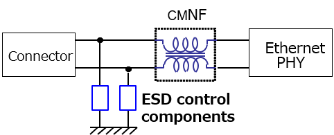
Component placement:(ESD_1)
Connector-ESD-CMNF-PHY
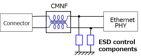
Component placement:(ESD_2)
Connector-CMNF-ESD-PHY
BCI Test method: Closed-loop method, injection current: 200 mA, frequency: 1 - 400 MHz
|
ESD control components |
Capacitance |
Operation start voltage |
Component placement |
Test results |
|---|---|---|---|---|
|
High Withstanding Type ESD Suppressors |
0.1pF typ. | DC:400~500V | ESD_1 | Pass |
| TVS diodes | 1.2pF typ. | VBR:11V | ESD_1 | Fail |
| TVS diodes | 1.2pF typ. | VBR:11V | ESD_2 | Pass |
This result is most likely due to the fact that TVS diodes, whose suppression operation start voltage is low at 11 V, eliminate a differential signal necessary for clamping noise in low voltage ranges, whereas high withstanding type ESD suppressors, whose suppression operation start voltage is 400 V or higher, pass a differential signal without clamping it.
Therefore, it was indicated that the use of TVS diodes as ESD control components necessitates their placement between the CMNFs and Ethernet PHY, as recommended by automotive Ethernet PHY vendors. On the other hand, it was confirmed that high withstanding type ESD suppressors can be placed directly under the connector.
Confirmation of Issue Resolution
This section will confirm that the two issues concerning the ESD control circuit recommended by automotive Ethernet PHY vendors can be resolved by the proposed circuit in which high withstanding type ESD suppressors are placed directly under the connector.
-
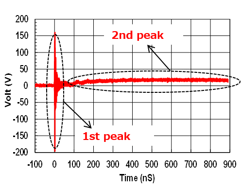
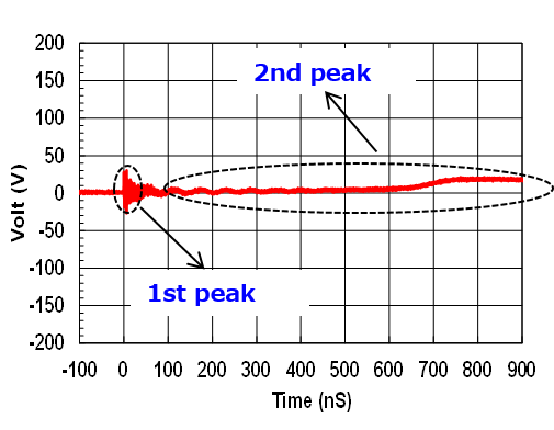
Decline in ESD protection effects for PHY (physical layer IC)1) Comparing ESD suppression characteristics of components aloneThe ESD suppression voltage waveforms (simulating voltages applied to the PHY IC that is to be protected) of ESD control components alone will be compared, also for the understanding of the basic characteristics of the ESD control components.
TVS diodes 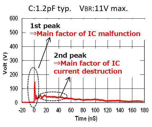
High Withstanding Type ESD Suppressors 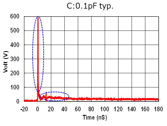
Evaluation method 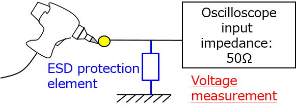
Evaluation condition:IEC61000-4-2
(150 pF - 330 Ω), contact discharge 8kV
Electrostatic Discharge Simulator: Noise Laboratory ESS-2002
Oscilloscope: Tektronix DPO7254As shown by the graphs, although the clamp voltages (voltages approx. 30 ns after the wave front value, corresponding to the 2nd peak) are nearly the same, the TVS diode indicates a lower peak voltage (voltages of the wave front values, corresponding to the 1st peak).
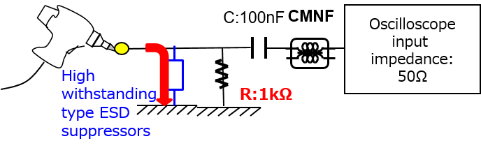
2) Comparing ESD suppression characteristics when the components are combined with a CMNFHere, a CMNF is added to the configurations for comparison as a condition similar to actual control circuits.
TVS diodes 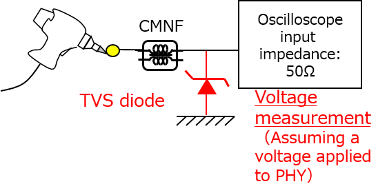
High Withstanding Type ESD Suppressors 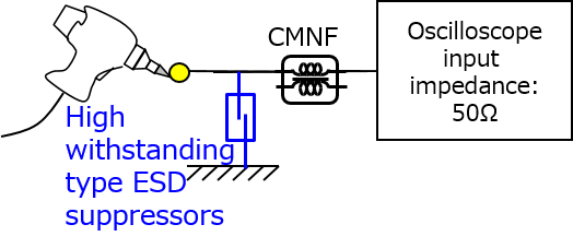
Evaluation condition: ISO10605 (330 pF - 2 kΩ), contact discharge 25 kV
lectrostatic Discharge Simulator: Noise Laboratory ESS-2002, Oscilloscope: Tektronix DPO7254The results confirmed that when a CMNF, which is necessary for circuit configuration, was included, the high withstanding type ESD suppressor indicated a lower 1st peak of the ESD suppression voltage waveform, thereby indicating that it was more effective than the TVS diode.
This is due to the following reason. In a circuit where a CMNF with a high impedance of about 1 - 10 kΩ was placed in the subsequent stage of the high withstanding type ESD suppressor, most of the ESD current flows to the ESD suppressor due to the high impedance of the CMNF. On the other hand, in a circuit with a TVS diode, where a CMNF is placed in an earlier stage, the CMNF does not contribute to passing the ESD current to the TVS diode.
In other words, in an ESD control circuit using a TVS diode, the TVS diode can only be installed between a CMNF and PHY, thereby decreasing the ESD protection effect for PHY. Using an ESD suppressor to place in an earlier stage of a CMNF (in fact directly below the connector) can effectively protect PHY. -
Degradation of terminal resistances R1 and R2 due to ESD
In actual circuits, terminal resistors exist at the connector ends. It is a well-known fact that resistors degrade due to ESD, and resistors need to be protected as part of ESD controls. Shown below are simulation circuits and ESD test results.
Evaluation condition: ISO10605 (330 pF - 2 kΩ),Contact discharges of ±15, ±20, and ±25 kV were applied 10 times each in a stepwise manner (total 60 times).
Sample resistors: Panasonic mass-produced products (surge-resistant products)ESD control components Resistance value change rate ΔR (%) Ave. Max. Min. TVS diodes (C: 1.2pF typ.) -2.70 -2.50 -2.90 High Withstanding Type ESD
Suppressors (C: 0.1pF typ.)-0.03 -0.02 -0.06 ESD was applied to each circuit, and the resistance value change rate of 1 kΩ terminal resistors was evaluated. The results indicated an approx. -3% change in the resistance value in the protection circuit using a TVS diode. This is assumedly because the ESD is directly applied to the terminal resistor, and the ESD current indicated by the red arrow flows to both the terminal resistor and TVS diode, causing the degradation of the resistor. The resistors used in the test were surge-resistant, and therefore, general products may undergo more significant degradation. Changes in the resistance value of the terminal resistor will cause the attenuation of the mode conversion amount Scd21, which indicates the conversion of part of differential signals to common mode noise, to decline.
The configuration using a high withstanding type ESD suppressor indicated a resistance value change rate of ±0.1% or less. This shows that because most of the ESD current can be passed to the high withstanding type ESD suppressor in the first stage, the terminal resistor can also be protected from ESD. These results indicated that to use a TVS diode as an ESD control component, it can only be placed between a CMNF and Ethernet PHY, as recommended by automotive Ethernet PHY vendors. On the other hand, it was confirmed that a high withstanding type ESD suppressor can be placed directly below the connector.
Summary of Automotive Ethernet ESD Controls
Automotive Ethernet is considered promising as a high-speed communication network for automotive ECUs toward achieving ADAS (advanced driver-assistance systems), etc. Meanwhile, its ESD control methods recommended by Ethernet PHY vendors have two issues, which are (1) decline in ESD protection effects for PHY (physical layer IC) and (2) degradation of terminal resistances R1 and R2 due to ESD.
To resolve these issues, this article proposed a protection circuit that uses high withstanding type ESD suppressors instead of a circuit configuration that uses TVS diodes. Even when placed directly under the connector, high withstanding type ESD suppressors, whose suppression operation start voltage is high, are resistant to malfunction due to noise, which is typically subject to the BCI Test. In combination with CMNFs, whose impedance is high, high withstanding type ESD suppressors can protect PHY devices more effectively than TVS diodes. Furthermore, since high withstanding type ESD suppressors can be installed directly below the connector, they can also protect the terminal resistors in subsequent stages, thereby being able to resolve the issues with the method recommended by Ethernet PHY vendors.
In addition, although it was not mentioned in this article, high withstanding type ESD suppressors have a very low capacitance of 0.1 pF and are therefore also compatible with the even more high-speed multi Giga (2.5 G/5 G/10 Gbps) communications, as well as to the automotive Ethernet standards 100BASE-T1 (transmission speed: 100 Mbps), 1000BASE-T1 (1 Gbps).
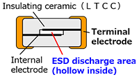
Differences between High Withstanding Type Suppressors and TVS Diodes
Finally, as part of basic knowledge, the differences between high withstanding type ESD suppressors and TVS diodes are shown below.
|
High Withstanding Type ESD Suppressors |
TVS Diodes (ZD) | |
|---|---|---|
| Structure |
 |
 |
|
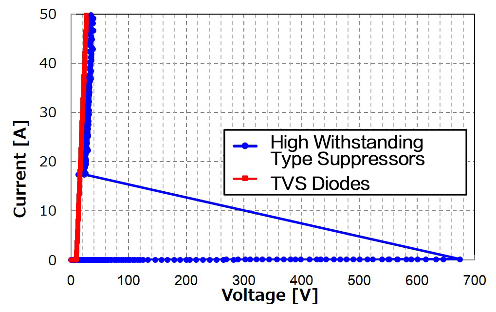
Voltage- current curve |
 |
 |
| Operating principle |
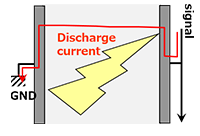 Arc discharge in the air in a hollow area |
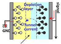 →It flows through the depletion layer when a high voltage is applied. |
| Features |
|
|
High withstanding type ESD suppressors obtain a high operating (trigger) voltage by using the air gap between the terminal electrodes. TVS diodes, which are basically Zener diodes, consist of a silicon PN junction, and the Zener voltage is the operating voltage. Although the voltage difference is fairly significant, the clamp voltage of high withstanding type ESD suppressors is almost equivalent with that of TVS diodes.
* Measurement condition: Hanwa Electronic Ind. HED-T5000-HC (large current TLP tester), pulse rise: 10 nsec,
pulse width: 100 nsec
Related product information
● ESD Suppressor